
|
|
Forum Index : PCB Manufacturing : Newbie on Kicad
| Author | Message | ||||
Dinosaur Guru Joined: 12/08/2011 Location: AustraliaPosts: 304 |
Hi All Installing KICad 7 on Debian 12 is like going through childbirth.  After going through the learning curve of using it, I managed to get to the point where I have a schematic and a circuit board. It is basically a two channel Volts to Freq. converter that is managed with a Rpi-Pico. When I exported to the PCB program it placed all components on the F.Cu side. So started placing tracks until all the spiders nest was gone. Then Google informed me that I should have drawn them on the B.Cu side. So, using properties, managed to transfer the tracks to B.Cu. Also drew the board outline on the Edge.Cuts layer. So, now getting the pcb made/etched/engraved. I use an engraver where I volunteer which has ArtCam and I am sure it is capable of isolation routing. But to get from KiCad to a gcode file is not as easy as installing various tools. With the latest Debian 12 , EVERYTHING is painful. I don't intend to make dozens of boards, so will pay to get a couple made.(any local offers ?) However, what I am not sure of, is when someone makes the PCB will I end up with a mirror image that is wrong.I assume that I am looking at B.Cu from the F.Cu side, as if the board was transparent. Also, it is a single sided board, but all the pads look like via's.(meaning double sided) I was hoping someone familiar with KiCad could look at the pic and give me some answers. Would be happy to send someone files if needed. 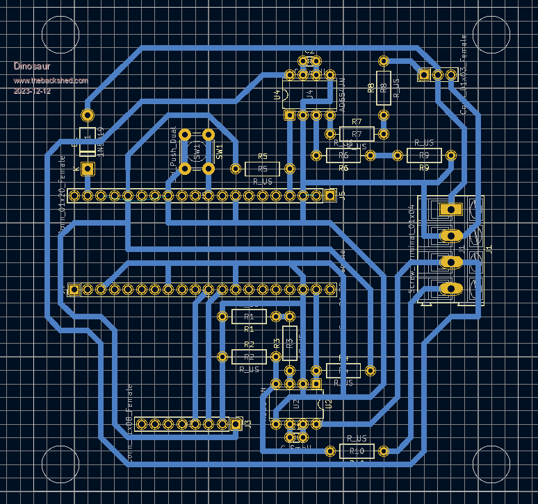 Regards Hervey Bay Qld. |
||||
| SunBakedWA Newbie Joined: 22/12/2023 Location: AustraliaPosts: 3 |
Hi, First time poster but have been using KICAD for over 10 years but I'm nowhere near an expert. I'm currently running on Linux Mint using the KICAD snap package and its all going good if that's any help for Debian. For a single layer board with components on the top and tracks on the bottom your plot looks fine. You are correct that, by default, the PCB is viewed from the top down as if the board were made of glass. In version 7 the default top copper track (F.Cu for front copper) layer is shown in red and the back (B.Cu for back copper) tracks are in blue. Anything that has both top and bottom copper will be yellow. As your using the library footprints and they have been designed for two layer boards they have both top and bottom copper tracks and so the through hole pads are all yellow. If you produce a single (bottom only) layer board then you just need to use the B.Cu layer gerber file. If you wanted you can use the board setup (PCB icon on the tool bar next to the floppy save icon) to remove the top layers in the board stack up but I don't think its worth it. You would normally produce gerber files for PCB manufacture by using the plot icon where the popup window allows you to select the layers you what. KICAD will produce a file for each layer - a layer being effectively a separate PCB manufacturing process so there's a front silk screen file, front solder mask file, a back copper file and so forth. You have to click on a separate button in the popup to produce the drill file. I have never used isolation routing, but when I have used a router to produce mechanical parts I have created the tool path gcode from a DXF file using a CAM program (ESTLCAM in my case). KICAD can directly output (plot in KICAD-ees) DXF files (and SVG files). When you click the plot icon; at the top left of the plot pop up window it says plot format with a drop down box. By default its set to gerber, but clicking on the drop down you can select DXF or SVG (among others). I would expect - again I haven't tried this directly - that the DXF plot could be loaded into the CAM software and a track outline selected as an 'on the line' route path to produce an isolation cut. The DXF would be as you see it on the screen so would need to be mirrored before you do the routing as you will be cutting with the bottom of the board upper most. I think ESTLCAM can flip the DXF file on import but as I say I have not done isolation routing as I go the gerber, zip file SEEED Studio / PCBWay / JLBPCB etc path (all not sponsored - I use SEEED around 5 to 7 times a year for different jobs and they have never let me down. That's just fact, not an advertisement!). It looks like your board is under 100mm square so you could get 10 for US$5 plus shipping from SEEED. The shipping is way more that the cost of the board production in my experience. BTW there is an option in the plot pop up window to mirror the output if you select a SVG file if that helps any? I hope this (apparently rather long) ramble helps out. All the best from WA. Everything here has been Sun Baked in WA |
||||
| Dinosaur Guru Joined: 12/08/2011 Location: AustraliaPosts: 304 |
Hi All Many thanks for your detailed reply. With the lack of interest in this thread, I HAD to spend weeks learning what you have detailed. For the single layer board I changed nearly all my components to SMD. As a result of that I used the F_Cu top layer as my routing "image" Days of googling found what I thought was great program "Line Grinder" https://www.ofitselfso.com/LineGrinder.php/ But it created a large circle of very dense routes in the middle of the gcode. No matter what I tried , couldn't get rid of it. Tried emailing, but after a day or two came back undeliverable. So, settled on KiCad --> .gbr plot --> gbr2ngc , then to view on an online simulation https://ncviewer.com/ Yesterday tried routing it onto a piece of laminated chip board, and it was so painfully slow. With gbr2ngc you can add g0 and g1 speed settings, so will try again after Christmas. With the sharp 30 degree routing bit, I was impressed with the accuracy and definition. The other item of interest was that Kicad draws a rather complex pad if that pad is in the middle of the gnd fill. These take a long time to route. So by editing the pcb footprint (not the library one) I could simply delete these pads as the legs of the components (or resistors) will solder directly onto the Gnd fill area. Even though I did not include the Edge Cuts layer in the plot, gbr2ngc will draw the outline of the board and the circles for hand drilling. The Rpi Pico headers were a bit more challenging, but by bending every pin left or right, I can surface mount the header and it will be quite stable. You can see the header footprint on the pic below, but minus the deleted pads. Anyway a long rant in reply, but I am ready to put this to copper. PS: Hope you are safe from the fires. 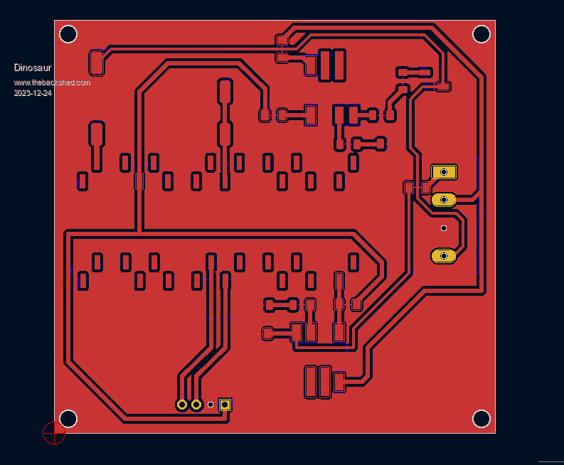 Regards Hervey Bay Qld. |
||||
Revlac Guru Joined: 31/12/2016 Location: AustraliaPosts: 961 |
Please don't write it up to a lack of interest, more like, interested but don't know anymore than you, I have tried Kicad but haven't gone far with it, so its still a learning curve for me.  Watching with interest.  Cheers Aaron Off The Grid |
||||
| Dinosaur Guru Joined: 12/08/2011 Location: AustraliaPosts: 304 |
Hi All Wasn't intended maliciously, just not much traffic on this subject and we all have our own priorities. Regards Hervey Bay Qld. |
||||
| Murphy's friend Guru Joined: 04/10/2019 Location: AustraliaPosts: 583 |
Just curious why anybody would use a router to make a PCB. Are there any advantages I cannot think of? My PCB's are etched by JLC PCB, they are cheap (especially in the 100 x 100mm format), they are cut to size, drilled with plated through holes and ready to use. Choosing their cheapest (and slowest) shipping option, they possibly would arrive way sooner that it'll take for me to figure out how to write a program for a router (if I had one ) to do this job.So, what am I missing? |
||||
| Dinosaur Guru Joined: 12/08/2011 Location: AustraliaPosts: 304 |
Hi All If you can't see what you are missing, then you are doing what you need. Me, well.... 1:Control freak I design it, I make it, buck stops with me. 2:If I don't have to put one cent in a Chinese pocket, I will be very happy. (very difficult, when soon my loaf of bread will come from there) Have a long tumultuous history with them. 3: The engraver is at the Historical Village & Museum where I volunteer. I do all the name badges and engrave items for sale by the museum. 4: Dates back to running a company involved in computerised weighing for 30 years, where the boards were drawn in autocad using poly lines and sent to local company. 20 years ago we had a single sided 20 bit A2D board, delivering 4000 samples per second, weighing diamonds at 3 per second. 5: Once proficient, I can design and make a board in hours. My wish: To have a laser etching head for the engraver. Look at some of the YouTube videos on this. Regards Hervey Bay Qld. |
||||
| Revlac Guru Joined: 31/12/2016 Location: AustraliaPosts: 961 |
I do like the idea of engraving and laser etching at home, there are many times when I need something done same day or a least test an idea before getting it done professionally, found the same with 3D printing and other things. Looking forward to see your results.  Hey, you have more Traffic now.  Cheers Aaron Off The Grid |
||||
Bryan1 Guru Joined: 22/02/2006 Location: AustraliaPosts: 1209 |
Well as a linux user myself I have tried a heap of ways to get my home made 3 axis router going and with using Kicad to first make some simple routines may be the first step. As to why engraving pcb's at home well if one has already made the tooling whynot just use it like it was done many years ago. It does seem now with mob's like JLCB and others it just too easy to kick the can down the road and take away that first step of making one's design come to life. Once I can readup on the CMM2 manual my first goal is write some code and just see if I get some life out the steppers on my router. I do have 3 off DM5566 (sp) stepper diver boards so basically it's just a enable, direction and step pulse so in theory it should just work. Now to be safe I'll make a poor mans isolated supply using some led's and see how it works. Well if one doesn't experiment one will never know what just can be done it one applies a bit of knowledge to keep those grey cells kicking on. Cheers Bryan |
||||
| Revlac Guru Joined: 31/12/2016 Location: AustraliaPosts: 961 |
Could use Inkscape to convert it, then on to laser etching or CNC there was a nice tutorial https://www.thebackshed.com/forum/ViewTopic.php?PID=144938#144938 Cheers Aaron Off The Grid |
||||
| SunBakedWA Newbie Joined: 22/12/2023 Location: AustraliaPosts: 3 |
That's the thermal relief. Its added to make soldering easier. The idea is main pad takes the solder and the little links to the surrounding copper plane limit the heat flow from the pad to the bulk mass of the plane when you solder the pin. They help to prevent you ending up with a dry joint or cooking the copper off the board. They also increase the electrical resistance between the component pin and the plane which can be significant at high frequencies when you have low voltage logic supplies...(oops wandered off topic again!) So long as you have a reasonably wattie soldering iron there absence shouldn't be a problem. I've always wanted to fabricate boards myself as it allows me to find out the circuit doesn't work much faster! Interesting you get good detail for surface mount by routing. That's good to know. I keep looking at the resin 3D printer in the garage and think its a hi DPI LCD panel with a UV light under it. Now just add software, UV sensitive Copper Clad, ferric chloride and the cats litter tray..... Everything here has been Sun Baked in WA |
||||
| Murphy's friend Guru Joined: 04/10/2019 Location: AustraliaPosts: 583 |
Thanks for explaining your reasons SunBaked, I understand now why. I started laying out PCB's 50 years ago when it was done with tapes & photography. Have stuck to the electronic version of this (much easier to correct) ever since it became available. As to Chinese manufacturing, I well remember when similar rejection was applied to stuff made in Japan. So much so that one was not allowed to park a Japanese made car outside a NSW RSL club. But the world moves on and I try to keep up with it. Have fun watching your router creating massive copper planes, isolated by tracks . What you need to do now is re- configure a 3D printer to print copper tracks onto a blank fibreglass board, are you up to that challenge  ? ? |
||||
| Dinosaur Guru Joined: 12/08/2011 Location: AustraliaPosts: 304 |
Hi All Someone is already doing that except with silver oxide and then baking it. I was not impressed with ragged edges of the tracks and pads. If the router has decent tolerances than I think it is still better then Laser. The videos I have seen seem to spend a lot of time tuning the power to prevent burning. With a 30 degree 3mm tapered cutter I am getting great results on fine text, so I am confident it will repeat that performance on the pcb. Start off slow so that you cut cleanly without tearing the copper. I will also edit the gcode file to get a deeper cut on the board outline. That will make it easy to simply break the bits off. I wont be using Levelling to be able to get even depth. My experience with the engraving has shown that very thin double sided tape glued directly to the alu bed works great. Even a tiny bubble in the tape shows up when you engrave small text. Discovered some of the pitfalls before even using a copper board. The isolation cuts converted into gcode use the diameter of your cutting tool to create the isolation, except that when the tool is small sharp and pointy. Then it wants to do multiple passes of the same section to get the width. Would take hours. So rigged the diameter of the tool with a command line switch -r 0.25 which made it only one pass. I can cut at any depth with the tool I use by setting it on the screen. Then it was repeating the radii on the pads as well, turned out the default for that was the same as the tool diameter. -F 0 fixed it, so that whatever radius is left over after a single cut is acceptable. The pic below is from NCViewer before I corrected the pad radius settings and you can clearly see the extra density corners where it spent a lot of time. 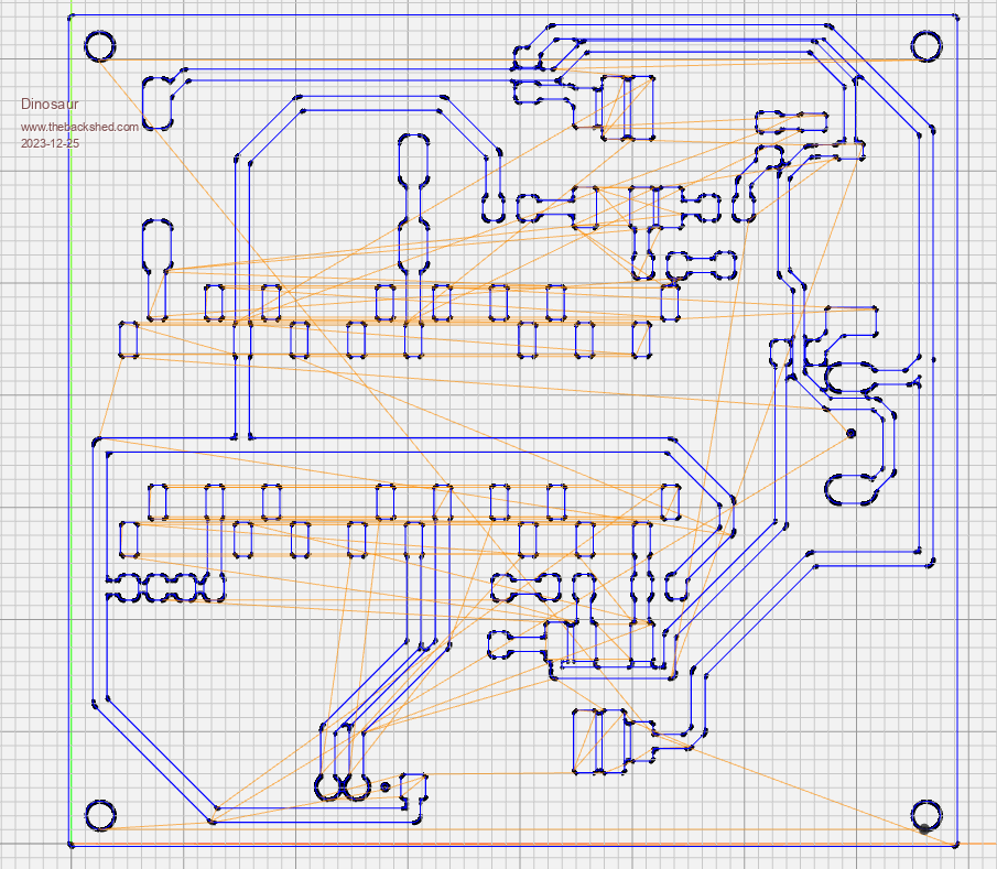 Regards Hervey Bay Qld. |
||||
| Dinosaur Guru Joined: 12/08/2011 Location: AustraliaPosts: 304 |
HI All Major setback. The engraver has spat the dummy. I moved in the X direction more then where the engraver was usually used. Motor stopped and made funny noises. Thought it was perhaps belt coming off, but when I tried to rotate by hand it was very tight. Once I got through that it was free all the way back and forth. But the motor would not run. Took the control box apart and checked each board for possible fuses.(that was hopeful for a Chinese machine) No visible evidence, so suspect the motor driver. Will ask the questions on Electronics thread. So no routing until fixed. Regards Hervey Bay Qld. |
||||
| Dinosaur Guru Joined: 12/08/2011 Location: AustraliaPosts: 304 |
Hi All Well that explains that.  Regards Hervey Bay Qld. |
||||
| SunBakedWA Newbie Joined: 22/12/2023 Location: AustraliaPosts: 3 |
Well, I have never seen that happen before! Everything here has been Sun Baked in WA |
||||
| Dinosaur Guru Joined: 12/08/2011 Location: AustraliaPosts: 304 |
Hi All The belt was very tight, which was not required as the belt was contained on the outside to prevent it from skipping a tooth. So side thrust on shaft plus an unexpected overload condition. Glad it was that though and not having to replace board that is no longer available, or replacing a 44 pin SMD motor driver. Edited 2023-12-27 11:31 by Dinosaur Regards Hervey Bay Qld. |
||||
| Dinosaur Guru Joined: 12/08/2011 Location: AustraliaPosts: 304 |
Hi All After persevering with the routing of PCB's for a few days now, have abandoned it. Learned some lessons that others treading this path may wish to heed. 1. Cutting tools are the biggest problem. The tapered 30 degree or 20 degree type work great for about half of the pcb, after which the edge goes off the cutter and it starts tearing the copper. You also have to go to deep to get say a 0.8mm isolation. If you go very slowly you may succeed, but I wasn't going to wait for 2 hours for a simple board. Tried a 0.8mm Titanium (coated ??) end mill and still had to go very slow, because it bends. Being an end mill and going in say 0.075 depth, you are using side cutting which causes tearing of the copper. 2. Table levelling. With more sophisticated programs you can accommodate an out of level table. I can't. Even a slight bubble in the very thin double sided tape causes problems, but that can be overcome. To get the table level, I would have to bolt on a block of wood and mill it level with a fly cutter, then put the pcb on top of it. 3. Board design A lot of time has to be spent on guaranteeing the gap for the cutter you intend to use. An isolation gap of 0.8mm ends up being 1.0mm (Bearing play, cutter bending etc) I also ended up simplifying the design knowing I had to cut it. Didn't want to drill any holes (except for terminals) so made it mostly surface mount. 4. Finished board. Hand Soldering components onto a board with a 0.8mm isolation gap is fraught with problems. Solder will bridge the gap and you spend more time cleaning it up. Never tried any drilling, but with a drill file converter to gcode that shouldn't be a problem. However in the end the mass of copper and the grooves all over the board made it look like Sh*t. Some of you may think (or say) "could have told you so" , but I now understand the router a lot better and also Kicad 7. So redesigned the board with all the features that I wanted on a double sided board and ordered it on-line (5 boards for $27) but the killer is the freight. Hervey Bay is a remote area apparently. Regards Hervey Bay Qld. |
||||
TassyJim Guru Joined: 07/08/2011 Location: AustraliaPosts: 5905 |
To solve the out of level problem, try autoleveller. http://www.autoleveller.co.uk/ I did a few boards a few years ago but other life matters got in the way and I have not got back to it yet. Maybe one day... Jim 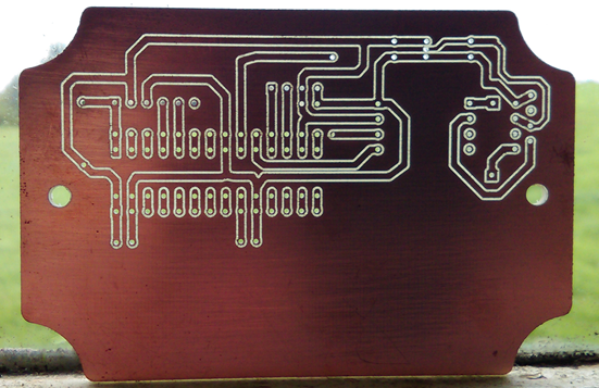 Edited 2024-01-04 15:28 by TassyJim VK7JH MMedit MMBasic Help |
||||
| Dinosaur Guru Joined: 12/08/2011 Location: AustraliaPosts: 304 |
Hi All Finished the board and tested, with great results. 2mA resolution and holding steady within 4 mA. The board takes about 10 minutes to settle on temperature and from then on it seems not to vary by more then 4mA. Made one mistake by forgetting to join the Pico Gnd to the Battery Negative, which meant each time I unplugged the usb cable the Pico died.A sharp eye will pick the jumper. Also the Power pack I was using to test it on my desk is above ground, which meant the counts were unstable until I jumpered it to ground. In the camper that won't happen as it is being powered by the Lipo4 battery. Soldering of the Shunt regulators is not pretty as I had to pump a lot of heat into it, so stopped as soon as I had a good connection. 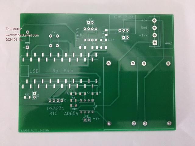 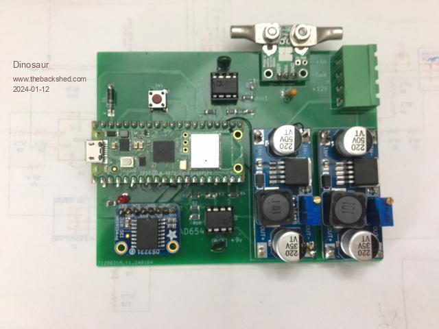 Regards Hervey Bay Qld. |
||||
